¶ title: Hostboard
description: Doc ID: 2022_AV_TN_HOSTBOARD
published: true
date: 2025-05-21T19:15:01.691Z
tags:
editor: markdown
dateCreated: 2022-04-29T10:33:55.963Z
¶ title: Hostboard
description: Doc ID: 2022_AV_TN_HOSTBOARD
published: true
date: 2024-12-30T21:18:50.336Z
tags:
editor: markdown
dateCreated: 2022-04-29T10:33:55.963Z
¶ title: Hostboard
description: Doc ID: 2022_AV_TN_HOSTBOARD
published: true
date: 2024-04-06T16:48:22.122Z
tags:
editor: markdown
dateCreated: 2022-04-29T10:33:55.963Z
¶ Hostboard
Version: R01
Reviewer: Thomas Pfeiffer
Review Date: 10.09.2022
Review status: 
¶ Table of Contents
¶ 1. Introduction
¶ 1.1 Purpose and motivation
For the past three years, the EPFL Rocket Team has been using the same STM32F446RE microcontrollers for its avionics. Because the product has reached its end of life and because of the increasing requirements for improved computing power, the choice has been made to develop a new hostboard with an improved microprocessor from the stm32mp1 series.
The purpose of this report is to explain the choices, design and manufacture processes we used to develop the hostboard for such a high speed processor. This report will take you through the steps of circuit design followed by the board design and finally board manufacturing and assembly.
¶ 1.2 Requirements
We define some requirements for this project. These requirements will guide the development choices of the project.
- The hostboard shall run a powerful and future proof microprocessor.
- The hostboard shall have a debug indicator.
- The hostboard shall have three extension slots for peripherals
- The hostboard shall have easy and accessible debug and programming ports.
- The hostboard shall have two CAN busses.
- The hostboard shall be able to measure the battery voltage.
- The hostboard shall be protected from ESD.
¶ 2. Reference Documents
| Ref | Description | Doc. ID | Issue |
|---|---|---|---|
| [RD01] | bottom text | ||
| [RD02] |
¶ 3. Definitions and Abbreviations
- ACI Atelier des Circuits Imprimés
- AV Avionics
- BOM Bill of Materials
- CA7 Cortex-A7
- CAN Controller Area Network
- CANFD Controller Area Network Flexible Data-Rate
- CM4 Cortex-M4
- DDR3 Dual Data Rate 3
- EMI Electromagnetic Interference
- eMMC Embedded MultiMediaCard
- EPFL Ecole Polytechnique Fédérale de Lausanne
- ERT EPFL Rocket Team
- ESD Electrostatic Discharge
- GUI Graphical User Interface
- HB Hostboard
- I2C Inter-Integrated Circuit
- LDO Low Dropout Regulator
- MPU Microprocessor Unit
- QFN Quad-Flat no-Leads
- RFI Radiofrequency Interference
- SDMMC Secure Digital and MultiMediaCard
- SDRAM Synchronous Dynamic Random Access Memory
- SPI Serial Peripheral Interface
- USB Universal Serial Bus
- UART Universal Asynchronous Receiver Transmitter
¶ 4. Concept Explanation
¶ 4.1 Method
¶ 4.1.1 Preliminary design
The purpose of this preliminary design is to asses and choose what is necessary for the STM32MP157 microprocessor to properly work. We will then decide how the components are laid out on the board and finally how the board is secured inside the rocket.
¶ 4.1.1.1 Hostboard
The STM32MP157 MPU needs memory and power. The memory will be provided in the form of a microSD card for storage and DDR3 SDRAM for the working memory. The power will be provided by a power management IC which is made for the STM32MP157 MPU.
In addition to that, we will have external interfaces for sensors and actuators as well as a dual CANFD bus for inter hostboard communication.
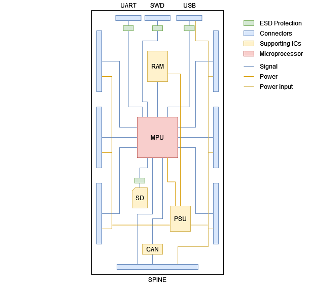
Block diagram of the hostboard's components and its connections.
The figure above shows a schematic representation of the different components of the hostboard. This also shows how the components will be laid out on the PCB.
At the center, there is the microprocessor, which is connected to the DDR3 SDRAM memory as well as to the microSD card storage. The central location is ideal for the processor as it will be connected to nearly all of the components and interfaces. The SDRAM is right next to the processor but far away enough such that the impedance controlled address and data buses can be properly routed.
The hostboard will also provide external peripheral connection points, which we will call sockets. There are three sockets on the front side of the board. They allow the attachment of three peripheral extensions per hostboard. The other connectors are for debugging on the top of the figure and for inter hostboard communication on the bottom in what we call the spine connector. The power input is also provided through the spine interface from the batteries.
Finally, we have the 5 V input which goes to the STPMIC1 and to the right hand side socket connectors. The STPMIC1 creates the necessary power supply rails for the MPU and it's peripherals. On the left hand side sockets, the power comes from the 3V3 output of the STPMIC1.
¶ 4.1.1.2 Structure
The structure serves to maintain the hostboards in place. The design of this structure is outside the scope of the project, however it is still relevant as the outline of the PCB must match this structure.
The Figure below shows a shematic representation of how the hostboards are attached as seen from the side. The red and blue component is the hostboard with its three extensions. It will be secured by two 3D printed rails on either of its sides and by mechanical stops on the top and bottom. This relieves the connectors from any stress due to the rocket's accelerations.
--- picture of the structure ---
¶ 4.1.2 Choice of components
The next step in our design process is to select the required components to support the microprocessor as well as our application. The choice of most components was motivated by their compatibility with our MPU, their availability and finally their price.
¶ 4.1.2.1 Microprocessor
The choice of microprocessor was motivated by a desire to stay in the STMicroelectronics ecosystem as we are already used to it. In the STM32 microcontrollers familly, there is only one series which combines the processing power of a dual core cortex-A7 processor with the real-time advantages of a cortex-M4 Microcontroller. It is the stm32mp157 serie. We specifically chose the stm32mp157dab1 due to its similarity with a relatively cheap development kit as well as the size and format of the BGA354 package which has the widest pitch. One big advantage of this processor is also its availability regardless of the current semiconductor shortage.
¶ 4.1.2.2 Power supply
As power supply we choose the recomended IC for this processor which is the STPMIC1APQR from stmicorelectronics. Sadly this exact model is not available, thus we buy the STPMIC1EPQR and reprogram it to meet our needs. This will require an additionnal I2C port to the hostboards, which is connected to the power supply.
¶ 4.1.2.3 Memory
The STM32MP157DAB1 microprocessor requires an external memory for its cortex-A7 cores. This memory will be a DDR3 SDRAM located next to the MPU. The choice of this memory was motivated by its similarity to the one used in the development kit as well as its backward compatibility to the slower speed of the MPU DDR3 controller. The exact model we use is the IS43TR16256B-125KBLI from ISSI.
¶ 4.1.2.4 Storage
The storage, also located outside the MCU will be handled by a microSD card. This is a temporary solution as unsoldered memory is not reliable enough in the high vibrations environment of a rocket flight. However, it is easier to program than soldered memory as it can be plugged into a computer. The plan for a later version is to use a soldered eMMC memory.
¶ 4.1.2.5 Can Transceivers
The CAN transceivers will transform the RX and TX signals from the MPU to the half duplex differential signal for the can bus.
The MAX3304 where chosen as they are some of the only which support 3V3 logic and are available.
¶ 4.1.2.6 Debug LED
To simplify the development of the avionics embedded software, the hostboards implement an RGB debug LED. The LED we choose is actually made of three LEDs covered by a opaque diffusing screen to mix the colors. We control these LEDs using PWM signals to mix the colors. To avoid using too much of the MPU's total output current, we drive the LEDs using a non inverting line buffer.
¶ 4.1.2.7 ESD Protection
In the past, we had some issues with the hostboards as they would often get broken by electrostatic discharge. This leads us to place ESD protections on the external connections of the new hostboards. We cannot place ESD protections everywhere as this takes too much space. However, we can place ESD protection where the user is most likely to touch exposed pads and connectors.
We use the RClamp0502A from Semtech which are versatile ESD protection circuits which also work on differential pairs.
On the microSD card connector, we use the EClamp2357NQ as we want to reduce ESD as well as EMI and RFI. The protection has an internal low-pass filter which removes EMI and RFI.
¶ 4.1.2.8 Connectors
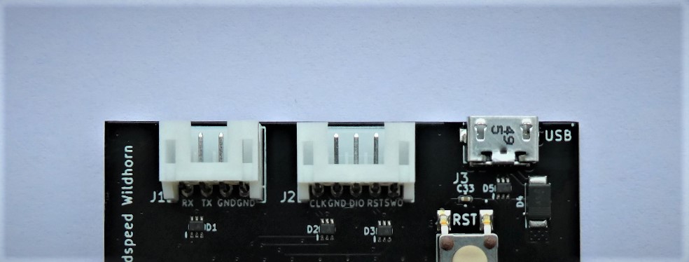
The connectors we use for debugging are two JST connectors and one micro USB. The JST and USB connector have a polarity, which prevents the user to plug them backwards.
For the socket and spine, we use simple pin strips as they are cheap and easily available. These connectors do not need to be structurally solid as the forces on them are handled by the structure.
¶ 4.1.3 Choice of interfaces
To interact with the external world, the hostboards have three main interfaces. The debug interface is designed to help during the development of the software. The socket interface allows the attachment of peripheral extensions. The spine interface allows for inter board communication and power delivery.
¶ 4.1.3.1 Debug
The debug interfaces will be used to diagnose problems during the software development as well as to download programs in the MPU's memory. For software diagnostics, we have the UART8 port. To download programs to the memory as well as to run the debugger, we use the SWD port.
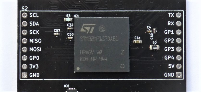
¶ 4.1.3.2 Socket
The Socket interfaces allow the connection to external peripherals such as sensors, telemetry or actuators. The hostboard has three socket interfaces and each interface is equipped with one USART, one I2C and one SPI port. Additionally, each interface has slightly different characteristics such as PWM channels, ADC inputs, DAC output or USB port.
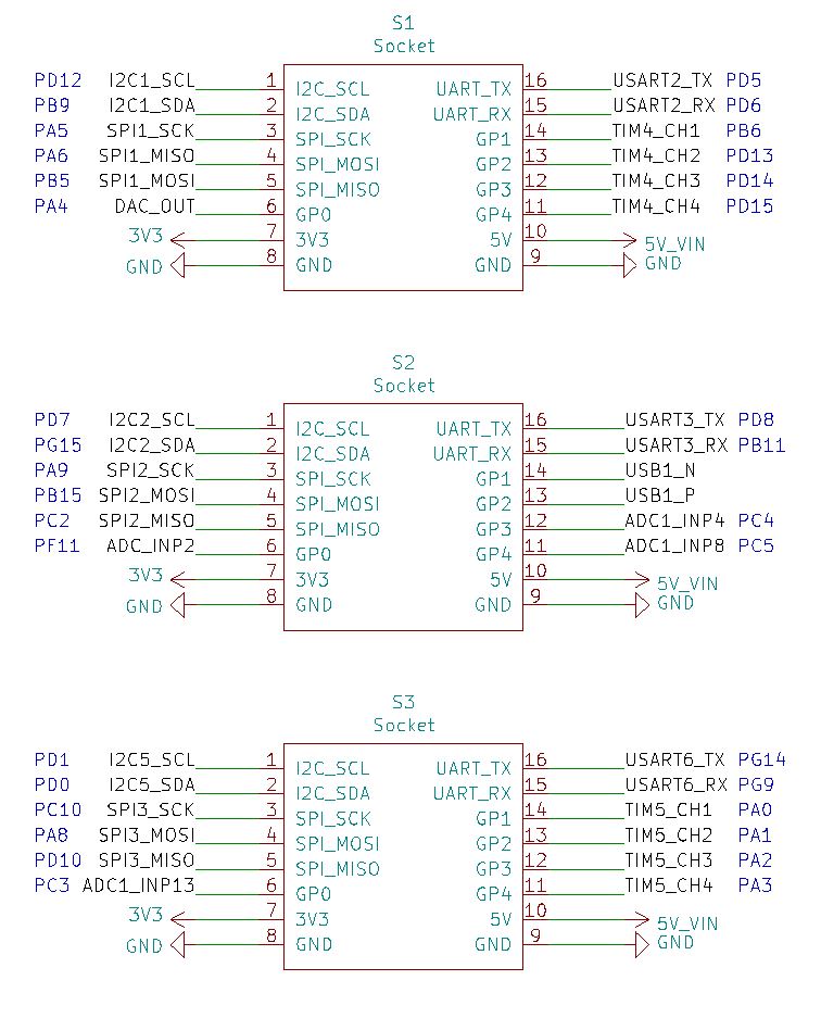
The Figure above shows the precise pinout of the three sockets. There, we can see what each socket has as additional interfaces.
The first socket has four timer channels, which are usually used as PWM outputs. It also has a DAC output, which can be used in combination with a buzzer to play sounds. All of these general purpose pins can also be used as simple GPIOs.
The second socket has an USB port, which might be useful if we want to connect an USB device such as a camera to the hostboards. The other general purpose pins are analog input, which can also be configured to be GPIOs. The particularity for the second socket is that the USB pins cannot be used for something else.
The third socket is very similar to the first as it also has four timer channels. In place of the DAC, it has an analog input which can also be used as GPIO.
¶ 4.1.3.3 Spine
The spine connector is used to connect multiple hostboards together as well as to connect the hostboards to the batteries.
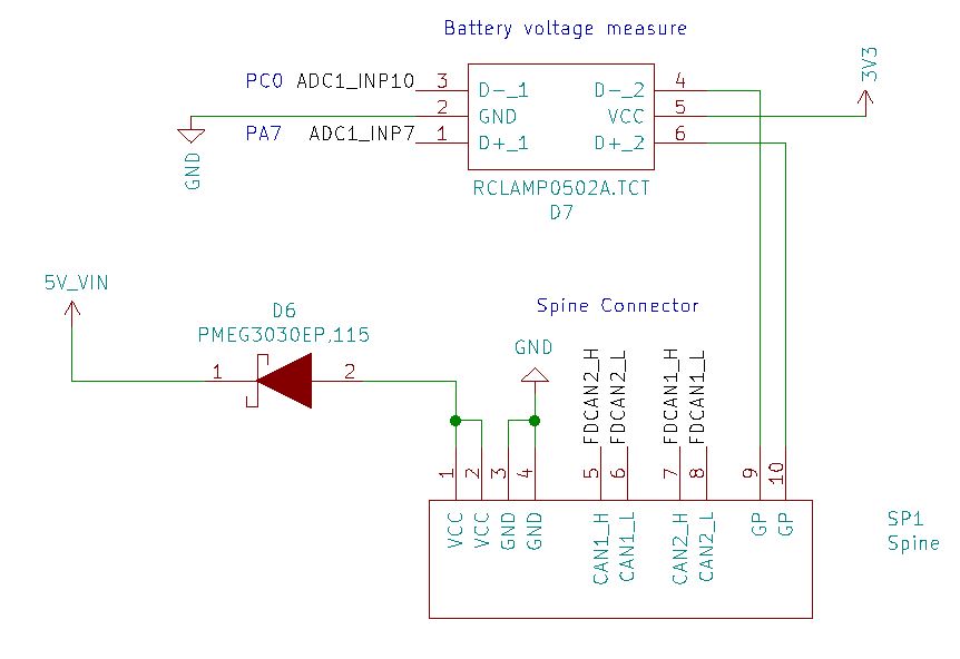
The connection between the hostboards is done through two redundant FDCAN buses. This will allow multiple hostboards to easily share and check data that they are processing. The redundant bus architecture allows us to implement and experiment on some transmission redundancy. This also allows us a larger bandwidth at the expense of redundancy.
The spine has two power and two ground pins for power delivery. It also has two connections to analog inputs. These will be connected to the batteries directly through voltage dividers in order to be able to sense the battery level.
The Figure above shows how the spine is connected internally. Note that the battery voltage measure pins are clamped in the 0 - 3.3 V range by the ESD protection diodes.
¶ 4.1.4 Circuit design
To simplify the circuit design and make the result easier to read, we separated it into five sheets. This section will go through these sheets and explain the choices that were made for the design of this circuit.
¶ 4.1.4.1 MPU
The MPU sheet holds all the signal connections to the MPU as well as the peripherals and interfaces.
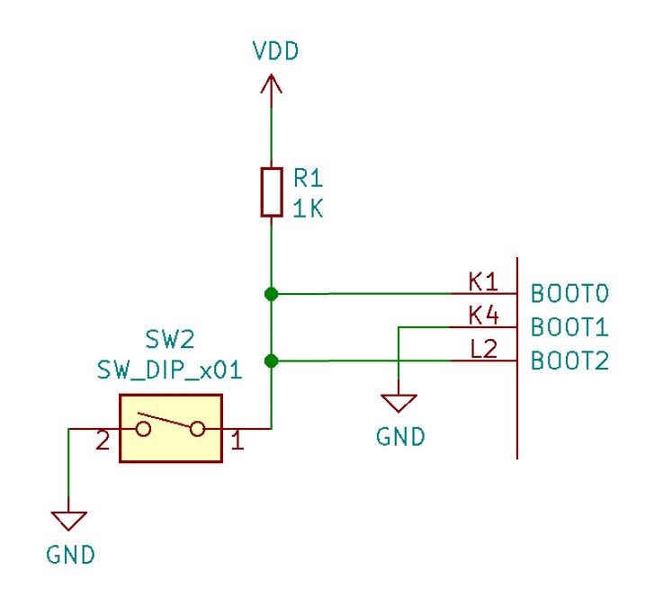
In order to select the proper boot mode for the MPU, we have hardwired two possible boot modes. These can be controller by a single dip-switch which shorts the BOOT 0 and 2 pins. In the shorted position, the MPU will boot from the USB or UART ports. In the open position, the MPU will boot from the microSD card.
Booting from USB or UART allows the user to load data into the memory from a computer or other host devices.
To provide the user with a convenient feedback on the program's operation and state, we implemented an RGB debug LED. The three channels of the LED are connected to three PWM outputs through non inverting buffers. These allow the LED to shine bright without using the limited current output capabilities of the MPU.
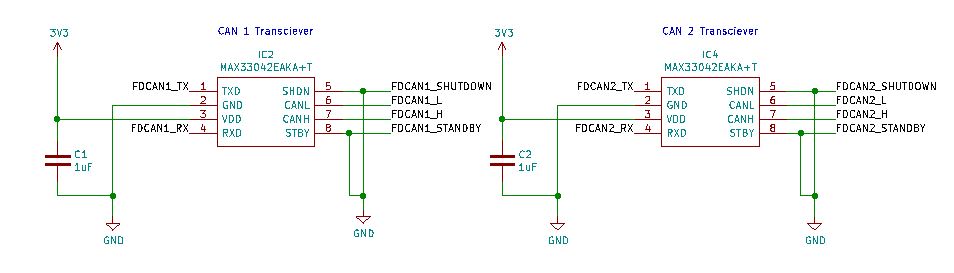
On this sheet are also the two FDCAN transceivers. They are connected to the MPU on one side and to the spine on the other side. Each one of them requires a decoupling capacitor. Their special functions shutdown and standby, which allow a lower power consumption, are not used in our application.
The debug ports are all connected through ESD protection circuits as these are the most likely to be touched or hot plugged. These are the UART8 serial port, the SWD debugger port and the USB2 port. The hostboard can be powered through the USB connector, but not the other debug interfaces.
¶ 4.1.4.2 MPU Power
The MPU POWER also holds the MPU connections, but this time only the ones related to power and the main decoupling for the MPU. This is done on a separate sheet as the MPU has a lot of power pins.
The MPU is powered by three main supplies VDD CORE, VDD DDR and VDD. These must be properly decoupled by capacitors. There are also some auxiliary supplies like VDD USB which must be connected to the VDD3V3 USBHS and VDD3V3 USBFS pins.
In addition to those main supplies, some power ports must be connected in the right way to configure the internal regulators. BYPASS REG1V8 must be grounded as we do not have an external 1.8 V regulator. VDD1V2 DSI PHY must be connected to VDD 1V2 DSI REG which in turn must be decoupled by a capacitor. All the regulator outputs must be decoupled by capacitors.
¶ 4.1.4.3 Memory
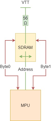
The DDR3 Sheet holds the connection between the MPU and the DDR3 SDRAM as well as the termination resistors network and its decoupling. The memory has three main connections to the processor, one address and two data buses.
These main connections are shown on the Figure below. In green, there is the address bus. This bus will be located on the bottom layer of the PCB and travels behind the memory chip. Additionally, it needs to have 56 termination resistors to the VTT DDR power supply. This power supply must be very stable and thus it has a huge amount of high frequency decoupling capacitors very close to the resistors.
In red, there are the two data buses byte 0 and 1. These will be located on the top layer of the PCB and travel on the left and right side of the memory chip. These data buses have the particularity of being swappable. The data bits inside of a byte are also swappable with the exception of the first bit which is used for calibration.
In our connection, the two bytes are swapped for convenience as well as a number of bits inside of the two bytes. This allows us to route every signal on one layer without a single intersection.
The last thing the memory needs is a power supply, which comes from VDD DDR. And we also have a reference power supply which is generated by the STPMIC1 at the half of VDD DDR.
¶ 4.1.4.3 Storage
The EMMC sheet holds the connection to the storage. For now, this is done using a microSD card which is simply connected through an ESD and RFI protection circuit. This is a quite straightforward connection directly to the SDMMC1 peripheral inside the processor.
¶ 4.1.4.4 Power
The POWER sheet holds the power supply subassembly. Here, everything revolves around the STPMIC1 power management IC.
The four main power rails are provided by four buck converters. These are VDD CORE at 1.2 V, VDD DDR at 1.5 V, VDD at 3.3 V and 3V3 at 3.3 V. The four synchronous buck converters need only an inductor and two capacitors as external components.
Three additional voltages are generated with LDO regulators. These are VREF DDR at 0.75 V, VREF DDR at 0.75 V and VDD USB at 3.3 V.
All the inductors and decoupling capacitor values are recommended from STM for the use of the STPMIC1 with our MPU in its configuration.
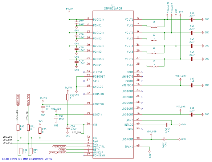
The Figure above shows how the power management IC is connected to the power rails and its necessary external passive components. On the bottom left side of the figure, there is the configuration port of the power supply. When the 0 resistors are unsoldered, this is connected to test points which can be used to externally reprogram the power supply. For normal operation of the hostboard, the resistors must be soldered. This will allow the microprocessor to reprogram the power supply if needed.
This configuration is done through an I2C interface. The following operations must be done in order to program the correct timings
- Write 0xEE at address 0xF8
- Write 0x92 at address 0xF9
- Write 0xC0 at address 0xFA
- Write 0x02 at address 0xFB
- Write 0xFE at address 0xFC
- Write 0xB0 at address 0xFD
- Write 0x02 at address 0xFE
- Write 0x01 at address 0xB9
It is then important to read those values in order to check that they where correctly registered as an incorrectly configured power supply might damage the microprocessor.
These operations can be made using any I2C master. We use a simple python program, located in appendix \ref{python}, which runs on a raspberry pi and uses it's GPIOs to connect to the STPMIC1. If we had a USB to I2C dongle, we could also use STM's user friendly GUI configuration tool to do it.
¶ 4.1.5 Board design
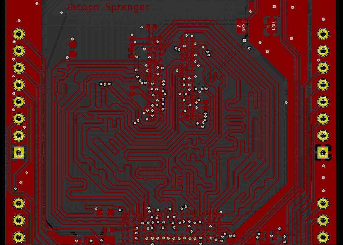
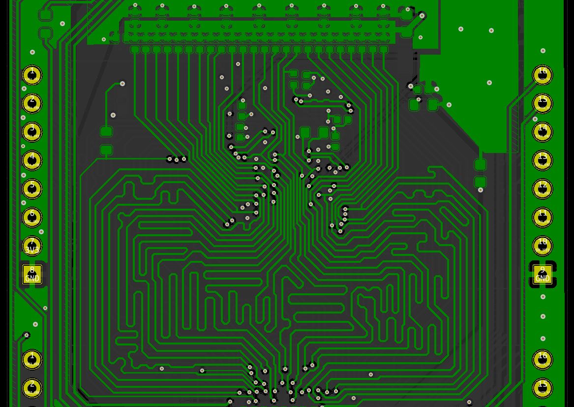
The largest part of this project is the board design. Once the circuit is done, we must transfer it to a physical medium, which in our case is a printed circuit board. This is quite challenging as all of the connections must fit on a limited number of planes without crossing each other. These signals must also be properly isolated from interfering with each other and they must sometimes follow specific guidelines in order to have the right electrical characteristics.
¶ 4.1.5.1 Design rules
The EPFL Rocket Team has a sponsoring agreement with PCBWay, thus they where chosen as manufacturer for the PCBs. We have to comply with their manufacturing capabilities, this will define the rules by which we design our circuit.
The first rule is the resolution of the copper etching. This gives us the minimum width and minimum space between two tracks. PCBWay can manufacture with this minimum at 4 mils for a reasonable price. This corresponds to 0.101 mm.
The second rule is the minimum size of the vias. PCBWay can manufacture vias with a diameter of 0.35 mm and a bore diameter of 0.2 mm.
These are the two main rules we followed during the board design.
¶ 4.1.5.2 PCB Stackup
The PCB stackup is the arrangement and allocation of the layers inside the circuit. For our use, we decided to go for a four layers PCB. This gives us a great compromise between ease of design, signal integrity and production cost.
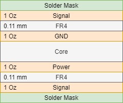
The details of our stackup can be seen on Figure \ref{fig:stackup}. The top and bottom layers are used for the signals. The first inner layer is a ground plane and the second inner layer is a power plane. These allow us to easily distribute the power throughout the board. Additionally the power and ground planes provide references and shielding for the impedance controlled signals.
The stackup also defines the distances between the copper planes. In our case, we have a 0.11 mm separation between the signal layers and their respective power plane. This is important as we will need it to compute the trace impedance as well as the required inter trace separation for an adequate signal integrity.
¶ 4.1.5.3 Controlled Impedance
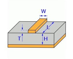
Some of our high speed signals such as the DDR3 connection or the USB need a controlled impedance in order to properly work. As we have a power and ground planes close to the signal layers, we route our impedance controlled tracks using microstrip lines and coupled microstrip lines. We use KiCAD to compute the parameters of the line in accordance with the desired impedance.
The DDR3 connection requires two types of signals with controlled impedance. The normal data and address lines, which are single ended, require a 55 impedance. This gives us a track with of W = 0.159 mm computed with KiCAD. The clock and data strobe lines, which are differential, require a 100 impedance. This gives us a track width of W = 0.188 mm and S = 0.323 mm of track separation.
The USB connection requires a single differential pair with an impedance of 90 . This connection thus requires a track width of W = 0.204 mm and S = 0.167 mm of separation.
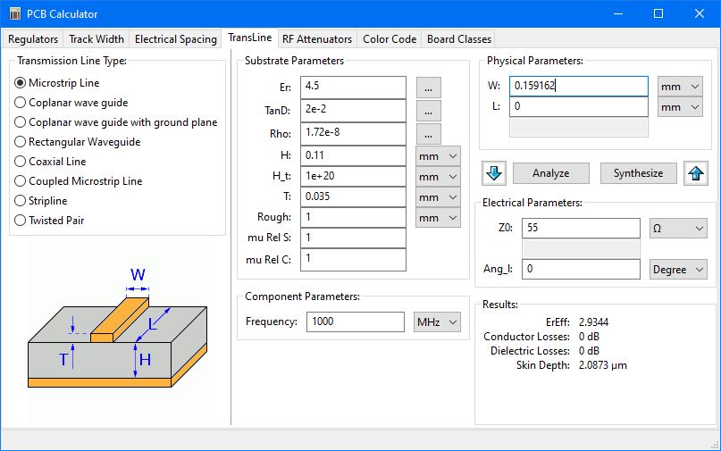
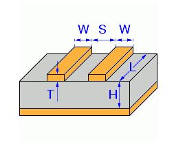
The Figure above shows how the impedance calculator looks like as well as its parameters for a microstrip line. It is very similar for a coupled microstrip line, with an additional output for the track separation. In our case, the height to the ground plane is H = 0.11 mm and the thickness of the copper is T = 0.035 mm because we have one ounce copper layers. The dielectric material is FR4, which has a dielectric coefficient of = 4.5.
¶ 4.1.5.4 Length matching
The second critical aspect for the DDR3 memory connection is the correct propagation time for the signals. This will be handled by closely matching the lengths of the signals which connect the processor to the memory.
The manufacturer provides some guidelines for the relative lengths of the tracks. In general, the signals should be closely matched inside a signal group with respect to the signal group's clock or data strobe. The longest signal must be the differential clock. The address lines must be closely matched to the clock from -1.016 mm to 0 mm of length difference.
The data strobes for the data bytes must be shorter than the clock for up to -15 mm. The data bytes must be closely matched to their respective data strobe for ±1.016 mm.
The manufacturer also gives us guidelines concerning signal integrity. The tracks must be separated of at least three times the distances to the ground plane as much as possible in order to avoid crosstalk. This means that our tracks must be separated of at least 0.33 mm. This is not possible everywhere, especially when approaching the fine pitch of the BGA. This guideline must however be respected as much as possible whenever it is possible. This guideline is called the 3S isolation rule.
To help the user respect these lengths and taking into account the internal pad to die lengths, the manufacturer provides a spreadsheet to check those lenght differences. This spreadsheet can be seen on the Figures \ref{fig:length_chart_a} and \ref{fig:length_chart_d} in the appendix \ref{ddr_appen}.
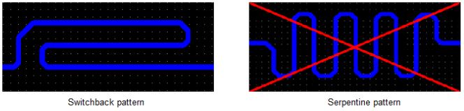
These spreadsheets only allow us to check that the track lengths are properly calibrated. However, we still need to route all those tracks between the processor and the memory. Additionally, we also need to manually tune the lengths by routing the tracks using serpentine and switchback patterns. The switchbacks are preferred over serpentine as they reduce the effect of orthogonal propagation. This effect makes the signals travel faster in a serpentine than in a straight line for the same track length, which is unwanted because we cannot control it accurately. The Figure \ref{fig:switchbacks} shows the difference between switchbacks and serpentines.
In order to route all of these tracks whilst respecting their desired lengths, the absence of crossings, their impedance as well as the 3S isolation rule. We need to come up with a methodology which allows us to tackle all of this constraints one by one to keep the routing manageable by a human.
The first step, as shown on the left of the Figure \ref{fig:routing_procedure}, is to perform an initial routing of all the tracks without any crossings. This allows us to define how we perform the BGA and what bits we swap to ease the routing. In this step, we do not care about the lengths of the traces, just their arrangement.
The second step, as shown on the right of the Figure \ref{fig:routing_procedure}, is to make each trace approximately at its final length. For now, we do not use the spreadsheet and only aim for tracks that are about 60 mm long. This length was chosen because it corresponds to the longest straight trace, thus we cannot make the connection shorter. This step allows us to determine how much space is needed by all the traces. This is the most difficult step as it requires the user to estimate the required space, then route all the tracks and finally see if the space was enough or too much. If there is not enough space, this must be started over by changing the initial estimation and potentially the lengths of the longest straight trace.
This iterative process can take up to several days in order to resolve all these length and space issues on all the memory connection buses. The best way is to start by the data buses as they will define the minimal length of the address bus.
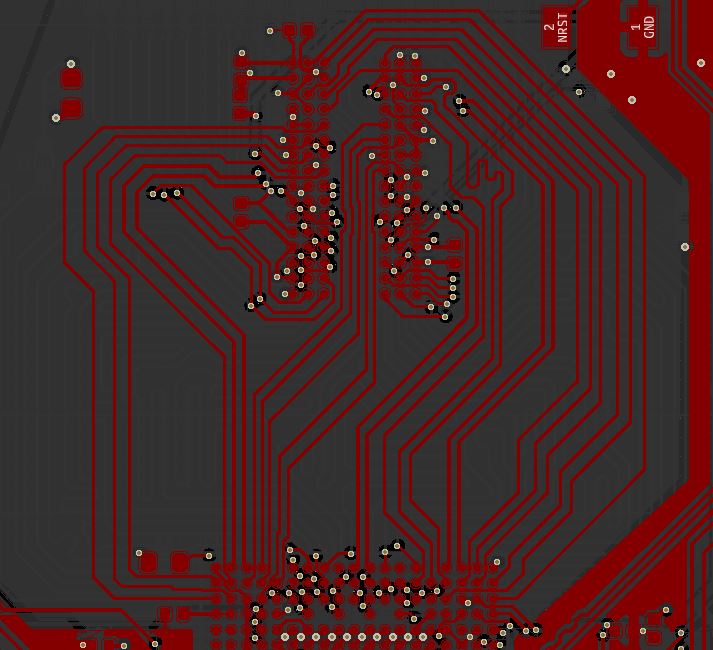
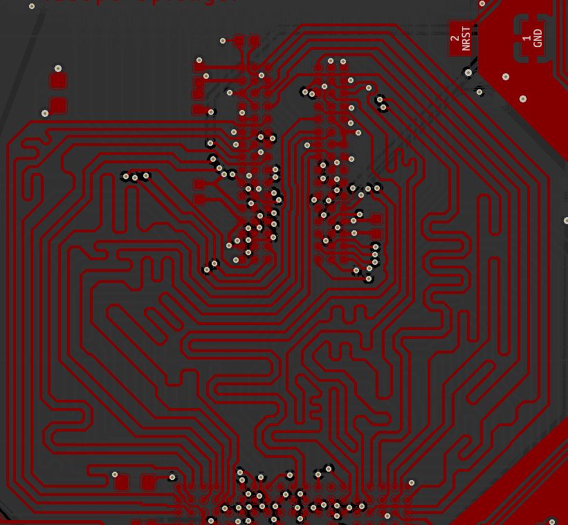
The final step, as shown in the Figure \ref{fig:routing_result}, is to finetune the track lengths using the spreadsheet. In this step, it is also good to check that the 3S isolation rule is respected as much as possible. This rule must also be respected inside the switchback and serpentine patterns to further reduce the risk of orthogonal propagation. This step is also quite time consuming as KiCAD only computes the track lengths and we also need to take into account the lengths of the vias as well as the lengths of the pad to die connections.
¶ 4.2 Results
¶ 4.3 Discussion
¶ 5. Conclusion
conclude, gg wp for writing this dope document.
Don't forget to notify the review team!